
Power and wavelength testing
Test the signal transmission strength and wavelength, ensure the signal decoding capability of the receiver, and maintain consistency in wavelength from the transmitter to the receiver.
已有账户?登录以快速结账。


Product Description:
Purely domestically produced components
● Transmission distance up to 2km
● Single power supply (3.3V)
● 2×5 SFF package SC interface
● Differential CML signal input and output
● SD output is an LVTTL signal
● Operating temperature: -40℃ to 85℃
● Complies with international safety standard IEC-60825 (Class 1 Laser)
Applications include
ATM 155Mbps,
SONET/SDH
100Mbps Ethernet equipment,
and other optical links.
Our strengths
lie in our advanced technology, extensive experience,
independent R&D and meticulous manufacturing, customizable
solutions with imported chips, stable performance,
comprehensive compatibility, and expert personnel to solve technical problems.
Our DDM digital diagnostic real-time monitoring module has undergone
specialized testing and verification, achieving satisfactory performance across all specifications.
Limiting conditions
| parameter | symbol | Minimum value | Maximum value | unit | Remark |
| Storage temperature | Ts | -40 | 85 | ℃ | – |
| Operating voltage | Vcc | -0.5 | 4.0 | V | – |
| welding temperature | – | – | 260 | ℃ | Welding time not exceeding 10 seconds |
| Input voltage | Vin | GND | Vcc | V | – |
Recommended conditions
| parameter | symbol | Minimum value | Typical value | Maximum value | unit |
| Operating voltage | Vcc | 3.1 | 3.3 | 3.5 | V |
| Operating temperature | Industrial grade | -40 | – | 85 | ℃ |
| working speed | – | – | 155 | – | Mbps |
| Operating current | Icc | – | – | 300 |
Transmission parameters (3.1V < Vcc < 3.5V)
| parameter | symbol | Minimum value | Typical value | Maximum value | unit |
| Optical parameters | |||||
| Optical power | Po(1310TX/1550RX) | -8 | – | 0 | dBm |
| Po(1550TX/1310RX) | -8 | – | 0 | ||
| wavelength | λC(1310TX/1550RX) | 1270 | 1310 | 1350 | nm |
| λC(1550TX/1310RX) | 1510 | 1550 | 1590 | ||
| Output spectral width | Δλ | – | – | 4 | nm(RMS) |
| Extinction ratio | ER | 10 | – | 1 | dB |
| Electrical parameters | |||||
| Differential input voltage | Vdiff_in | 200 | – | 1000 | mV |
| transmit enable input voltage | Disable | 2 | – | VCC | V |
| Enable | 0 | – | 0.8 | V | |
Receive parameters
| parameter | symbol | Minimum value | Typical value | Maximum value | unit | Remark |
| Optical parameters | ||||||
| Sensitivity | Sen | – | – | -34 | dBm | 1 |
| saturation | PMAX | -3 | – | – | dBm | |
| (Recovery) Signal Detect — Asserted | Pa | – | – | -35 | dBm | |
| (Disable) Signal Detect — Deasserted | Pd | -50 | – | – | dBm | |
| (Hysteresis) Signal Detect — Hysteresis | Phys | 1 | – | 4 | dB | |
| center wavelength | λ(1310TX/1550RX) | 1500 | 1550 | 1600 | nm | |
| λ(1550TX/1310RX) | 1260 | 1310 | 1360 | |||
| Electrical parameters | ||||||
| Differential output voltage | Vdiff_out | 300 | – | 800 | mV | |
| Receive SD indication voltage | Normal | 2.0 | – | Vcc | V | |
| LOS | 0 | – | 0.8 | V | ||
Notes: 1. Test values are average optical power; BER < 10⁻¹², PRBS 231⁻¹;
Pin Definitions
| Serial Number | name | Input/Output Types | describe |
| 1 | RX_VEE | enter | Receiving location |
| 2 | RX_VCC | enter | +3.3V receiving power supply |
| 3 | SD | Output | The signal level is LVTTL, indicating that a signal has been received and a low level indicates that no signal has been received. The module has a built-in pull-up resistor. |
| 4 | RD- | Output | Receive inverting output, AC coupled, CML level output |
| 5 | RD+ | Output | Receive positive output terminal, AC coupled, CML level output |
| 6 | TX_VCC | enter | +3.3V transmitting power supply |
| 7 | TX_VEE | enter | launch site |
| 8 | Tx_Dis | enter | Transmit enabled is achieved by a built-in pull-up resistor in the module. The signal level is LVTTL, and its states are: Low: Transmit on; High: Transmit off. |
| 9 | TD+ | enter | Transmit positive input, AC coupled, CML level input |
| 10 | TD- | enter | Transmitter inverting input, AC coupled, CML level input |
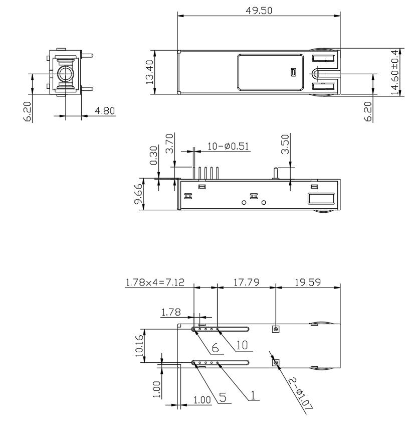
Product Dimensions
Test the signal transmission strength and wavelength, ensure the signal decoding capability of the receiver, and maintain consistency in wavelength from the transmitter to the receiver.

Test the bit error rate and packet loss rate, to make them meet the corresponding standards and ensure the performance of transceivers.

Test the transceivers' eye diagram situation, receiving sensitivity, extinction ratio, wavelength, light-emitting, light-receiving, current and voltage, to ensure the signal quality, stability and reliability of the transmission.

Check the end face of the transceivers and keep them clean for more stable data transmission, better performance, and durability.

Every module is quality tested for compatibility in the multi-brand switches environment, guaranteeing flawless operations.