Описание продукта
FT7606BSTZ-xx — это 16-битная 8-канальная система синхронного выборочного преобразования и сбора данных (DAS, Data Acquisition System). Каждый прибор оснащен встроенной защитой входов от зажима (клемпинга) аналоговых сигналов, вторым порядком фильтром антиалиасинга, усилителем с хранением и отслеживанием, 16-битным аналого-цифровым преобразователем (АЦП) с зарядовым перераспределением по принципу последовательного приближения, гибким цифровым фильтром, источником опорного напряжения 2,5 В, буфером опорного напряжения, а также высокоскоростными сериализованными и параллельными интерфейсами.
FT7606BSTZ-xx питается от одиночного источника напряжения 5 В и способен обрабатывать истинно двуполярные входные сигналы ±10 В и ±5 В. При этом все каналы могут выполнять выборку с скоростью пропускания до 200 кспс (килобайт выборок в секунду). Циркуит защиты от зажима входных сигналов耐受ет напряжение до ±16,5 В. Независимо от частоты выборки входное аналоговое сопротивление FT7606BSTZ-xx составляет 1 МОм. Благодаря работе от одиночного источника напряжения, встроенному фильтру и высокому входному сопротивлению для устройства не требуются драйверные операционные усилители и внешние двуполярные источники питания.
Частота среза 3 дБ фильтра антиалиасинга FT7606BSTZ-xx равна 45 кГц. При частоте выборки 200 кспс фильтр обеспечивает характеристику подавления антиалиасинга 46 дБ. Гибкий цифровой фильтр, управляемый по выводам, позволяет улучшать соотношение сигнал/шум (ССП, SNR) и снижать полосу пропускания 3 дБ.
Особенности микросхемы
- Работа от одиночного источника питания: +2,5 В до +5,5 В
- 8 синхронных входов для выборочной регистрации
- Диапазон истинно двуполярных аналоговых входов: ±10 В, ±5 В
- Один аналоговый источник питания 5 В; диапазон VDRIVE (напряжение для драйвера): 2,3 В до 5 В
- Защита аналоговых входов от зажима (клемпинга)
- Входной буфер с аналоговым входным сопротивлением 1 МОм
- Аналоговый фильтр антиалиасинга второго порядка
- Встроенное высокоточное опорное напряжение с буфером; температурный коэффициент дрейфа: 5 ppm/°C
- 16-битный АЦП (аналого-цифровой преобразователь) со скоростью 200 кспс (килобайт выборок в секунду) для всех каналов
- Функция перевыборки (оверсэмплинга) посредством цифрового фильтра
- Гибкие параллельный/сериализованный интерфейсы, совместимые с SPI/QSP/MICROWIR/DSP
- Рейтинг ЭПР (электростатического разряда) 7 кВ для аналоговых входных каналов
- Параметры входных каналов: ССП (соотношение сигнал/шум) 89 дБ, ТГД (треугольное гармоническое искажение) −106 дБ
- Погрешность интегрального нелинейности (INL): ±0,5 ЛСБ; погрешность дифференциального нелинейности (DNL): ±0,5 ЛСБ
- Низкое энергопотребление: 130 мВт; режим ожидания: 35 мВт
- Температурный диапазон работы: −40°C до +85°C / −40°C до +125°C
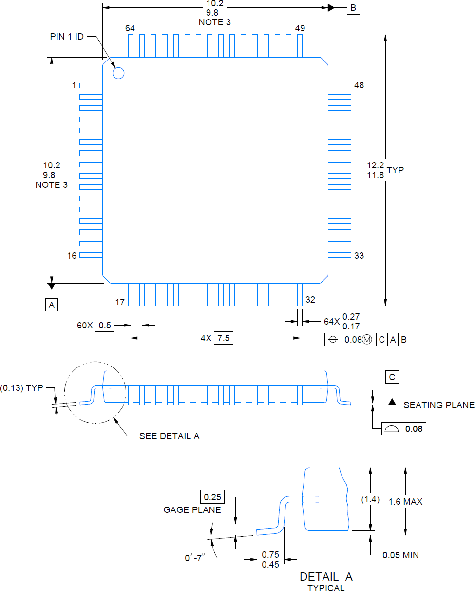
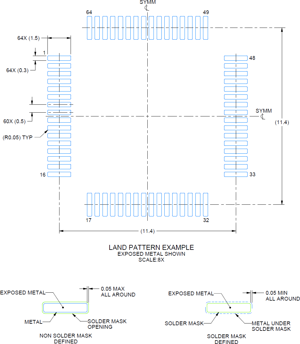
- Корпус 64-контактный LQFP (малогабаритный кварцевый плоский корпус с выводами по периметру)
Применение
- Управление многофазными электродвигателями
- Системы мониторинга и защиты силовых линий
- Приборы и системы управления
- Многоосевые системы позиционирования
- Системы сбора данных (DAS, Data Acquisition System)
Functional Block Diagram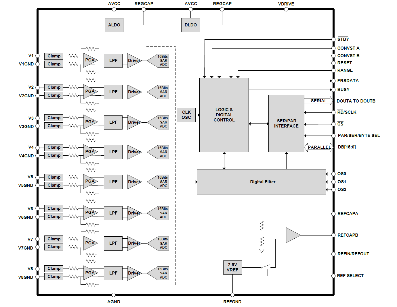
Figure 1. Functional Block Diagram
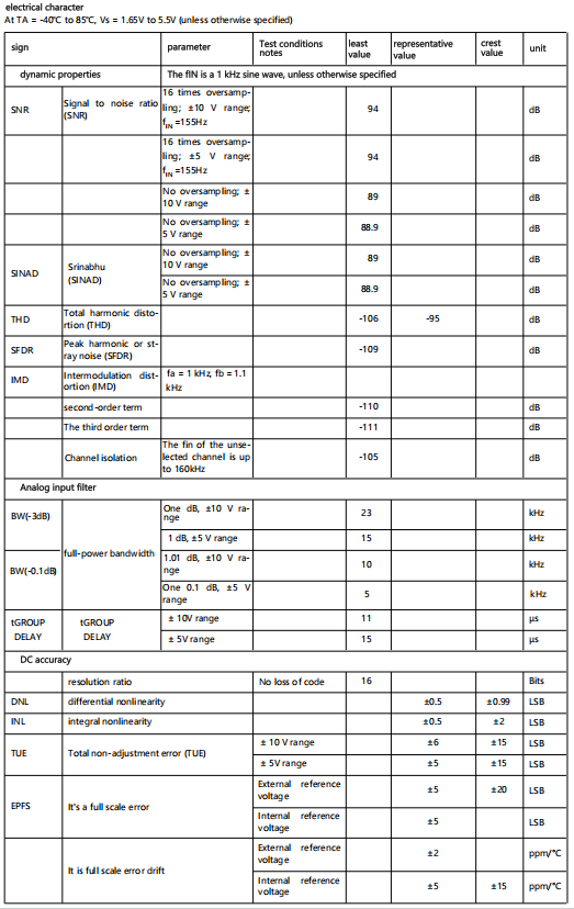
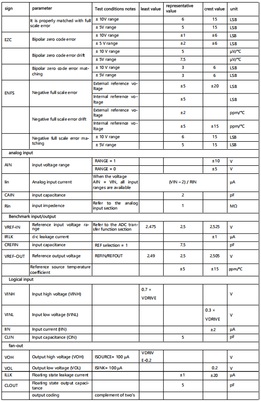
Electrical Characteristics
Timing Specifications
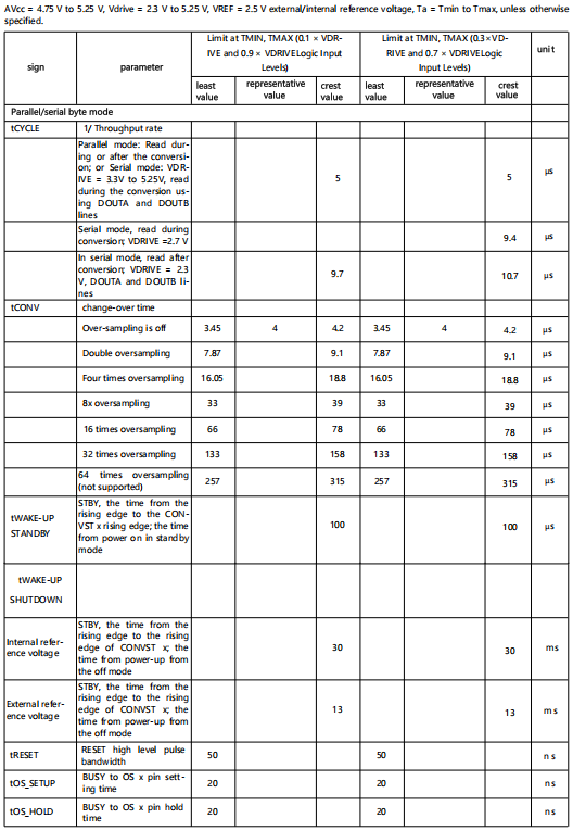
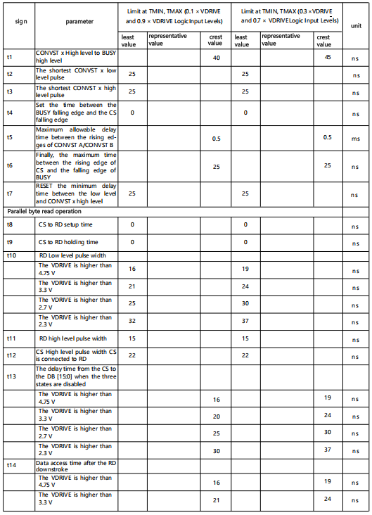
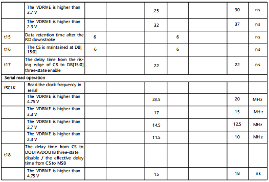
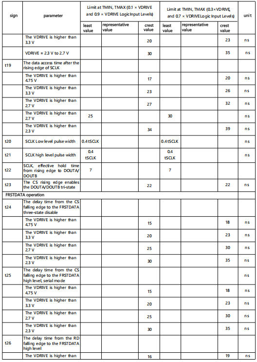
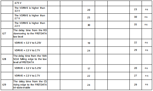
Timing Specifications
Figure 2. CONVST Timing – Read After Conversion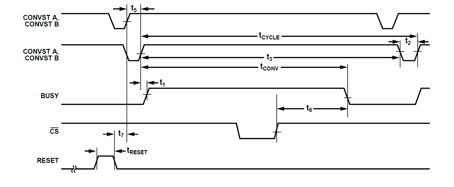
Figure 3. CONVST Timing – Read During Conversion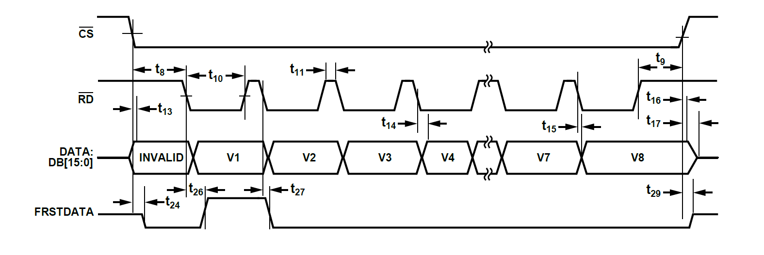
Figure 4. Parallel Mode with Independent CS and RD Pulses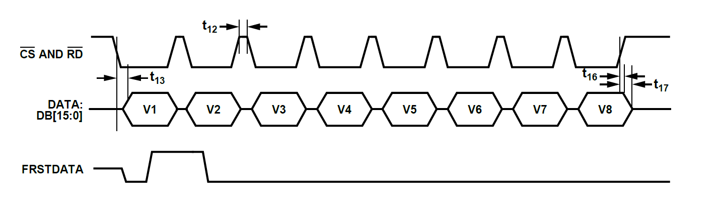
Figure 5. Parallel Mode with CS and RD Connected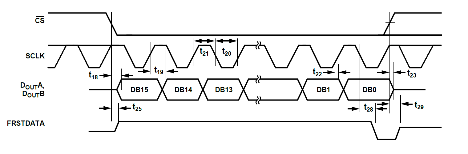
Figure 6. Serial Read Operation (Channel 1)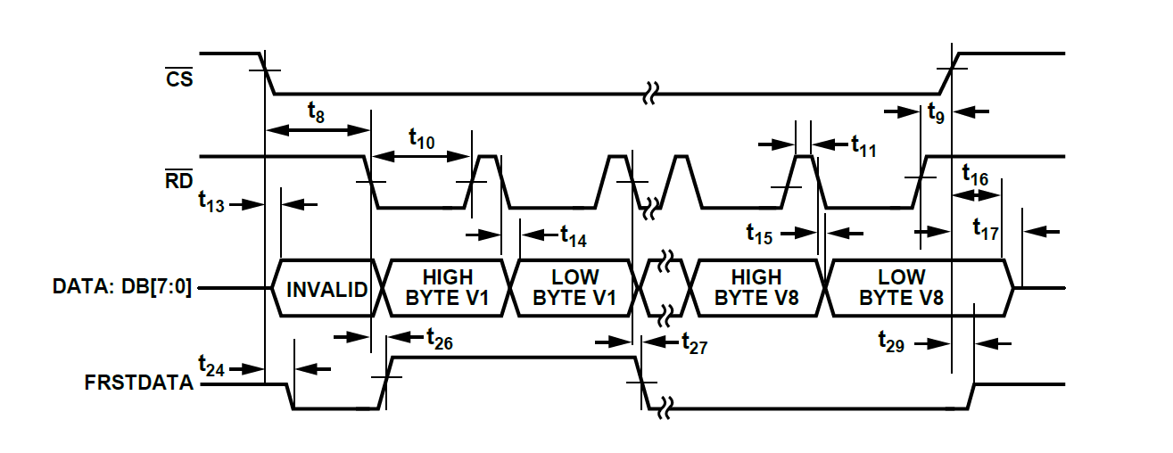
Figure 7. Byte Mode Read Operation
Pin Configuration
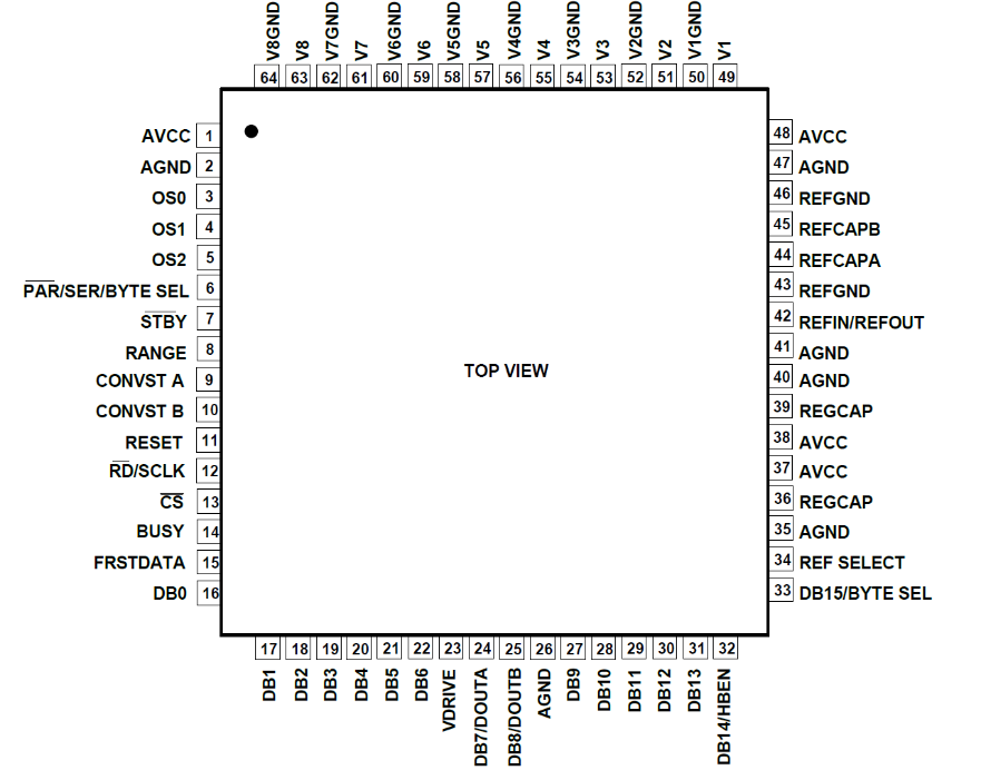
Figure 8. Pin Configuration
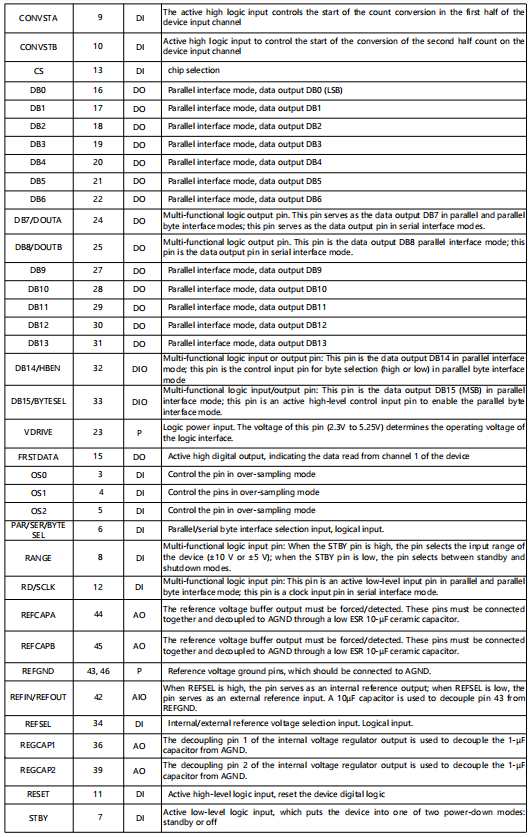
Table 1. Pin Function Definitions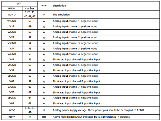
Detailed Description
Converter Overview
The FT7606BSTZ-xx is a data acquisition system that employs a high-speed, low-power, charge redistribution successive approximation analog-to-digital converter (ADC) and allows simultaneous sampling of 8 analog input channels. The analog inputs on the FT7606BSTZ-xx can accept true bipolar input signals. The RANGE pin enables selection of ±10 V or ±5 V input ranges. The FT7606BSTZ-xx is powered by a single 5V power supply.The FT7606BSTZ-xx integrates built-in input clamp protection, input signal scaling amplifiers, second-order anti-aliasing filters, sample-and-hold amplifiers, an on-chip reference voltage source, a reference voltage buffer, a high-speed ADC, digital filters, as well as high-speed parallel and serial interfaces. Sampling on the FT7606BSTZ-xx is controlled using the CONVST signal.
Analog Inputs
● Analog Input Range
The FT7606BSTZ-xx is capable of handling true bipolar, single-ended input voltages. The logic level on the RANGE pin determines the analog input range for all analog input channels. If this pin is connected to a logic high level, the analog input range for all channels is ±10 V. If the pin is connected to a logic low level, the analog input range for all channels is ±5 V. A logic change on this pin has a direct impact on the analog input range; however, in addition to the normal acquisition time requirements, there is typically a settling time requirement of approximately 80µs.It is recommended that the RANGE pin be set via hardwiring according to the input range required by the system signals. During normal operation, the applied analog input voltage should be maintained within the analog input range selected via the RANGE pin. A RESET pulse must be applied after power-up to ensure that the analog input channels are configured to the selected range. During power-down, it is advisable to tie the analog inputs to GND.As per the analog input clamp protection section, overvoltage clamp protection is recommended for transient overvoltage conditions and should not remain active for an extended period. It is emphasized that analog inputs outside the conditions mentioned herein may degrade the bipolar zero-code error and THD performance of the FT7606BSTZ-xx.
● Analog Input Impedance
The FT7606BSTZ-xx features an analog input impedance of 1MΩ. This is a fixed input impedance that does not vary with the sampling frequency of the FT7606BSTZ-xx. Such a high analog input impedance eliminates the need for a driver amplifier in front of the FT7606BSTZ-xx, allowing direct connection to signal sources or sensors. Since no driver amplifier is required, bipolar power supplies (which are typically noise sources in the system) can be removed from the signal chain.
● Analog Input Clamp Protection
Figure 9 presents the analog input structure of the FT7606BSTZ-xx. Each analog input of the FT7606BSTZ-xx incorporates a clamp protection circuit. Despite being powered by a single 5V power supply, this analog input clamp protection allows input overvoltage up to ±16.5 V.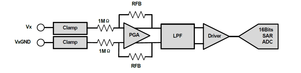
Figure 9. Analog Input Circuit
Figure 10 illustrates the voltage-current characteristics of the clamp circuit. When the input voltage does not exceed ±16.5V, no current flows through the clamp circuit. For input voltages above ±16.5V, the on-chip clamp circuit is activated.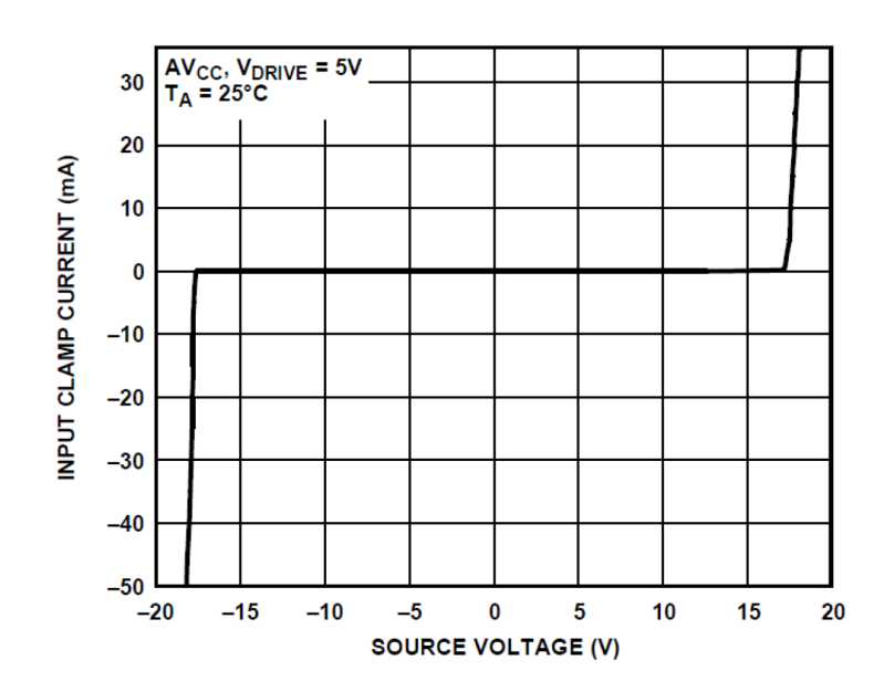
Figure 10. Input Clamp Protection Characteristics
A series resistor should be placed on the analog input channel to limit the current to ±10mA when the input voltage exceeds ±16.5V. If there is a series resistor on the analog input channel Vx, a corresponding resistor is required on the analog input GND channel VxGND (see Figure 11). Without a corresponding resistor on the VxGND channel, an offset error will occur on that channel.It is recommended to employ an input overvoltage clamp protection circuit to protect the FT7606BSTZ-xx from transient overvoltage events. It is not advisable to leave the FT7606BSTZ-xx in a state where the clamp protection circuit is active during normal operation or prolonged power-down, as this may degrade the bipolar zero-code error performance of the FT7606BSTZ-xx.
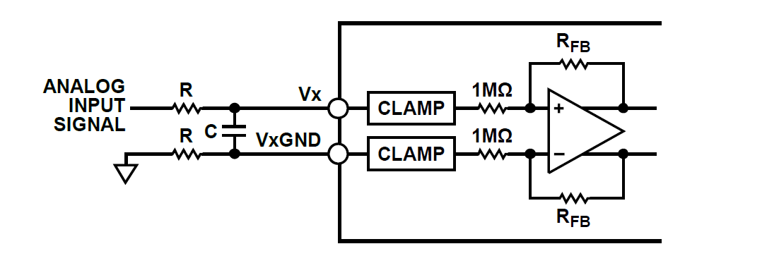
Figure 11. Input Resistance Matching on Analog Inputs
● Analog Input Anti-Aliasing Filter
The FT7606BSTZ-xx also incorporates an analog anti-aliasing filter. In the ±5 V range, the -3 dB frequency is typically 22 kHz. In the ±10 V range, the -3 dB frequency is typically 45 kHz.
ADC Transfer Function
The output coding of the FT7606BSTZ-xx is two’s complement. The designed code transition occurs between consecutive integer LSB values, specifically between 1/2 LSB and 3/2 LSB. For the FT7606BSTZ-xx, the LSB size is FSR / 65,536. The ideal transfer characteristic of the FT7606BSTZ-xx is shown in Figure 12. The size of the LSB depends on the selected analog input range.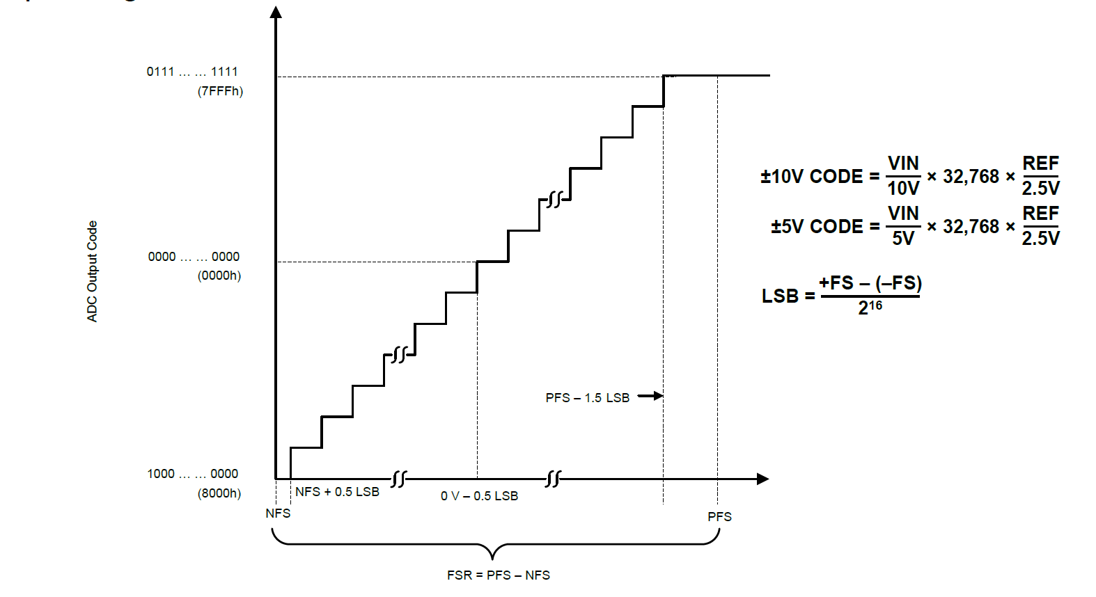
Figure 12. Transfer Characteristics
| +FS | MIDSCALE | -FS | LSB | |
| ±10V RANGE | +10V | 0V | -10V | 305µV |
| ±5V RANGE | +5V | 0V | -5V | 152µV |
Internal/External Reference Voltage
The FT7606BSTZ-xx incorporates an on-chip 2.5V bandgap reference. The REFIN/REFOUT pin allows access to the 2.5V reference, generates an on-chip 4.0V reference internally, or enables a 2.5V external reference to be applied to the FT7606BSTZ-xx. An externally applied reference voltage of 2.5V can also reach 4.0V using the internal buffer. This 4.0V buffered reference is the one used by the SAR ADC. The REFSELECT pin is a logic input pin that allows users to select between the internal reference and external reference. If this pin is set to logic high, the internal reference is selected and enabled. If the pin is set to logic low, the internal reference is disabled, and an external reference voltage must be applied to the REFIN/REFOUT pin. The internal reference buffer is always enabled. After reset, the FT7606BSTZ-xx operates in the reference mode selected by the REFSELECT pin. Both the internal and external reference options require decoupling of the REFIN/REFOUT pin. A 10µF ceramic capacitor is required on the REFIN/REFOUT pin. The FT7606BSTZ-xx includes a reference buffer that can boost the REF voltage to approximately 4.0V, as shown in Figure 13. The REFCAPA and REFCAPB pins must be externally shorted together and connected to REFGND with a 10μF ceramic capacitor to ensure the reference buffer operates in a closed-loop configuration. The reference voltage at the REFIN/REFOUT pin is 2.5V.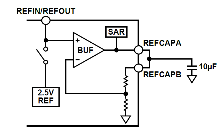
Figure 13. Reference Voltage Circuit
When the chip is configured in the external reference mode, the REFIN/REFOUT pin functions as a high-input-impedance pin. For applications utilizing multiple FT7606BSTZ-xx devices, the following configurations are recommended based on application requirements:
● External Reference Voltage Mode
An external reference can be used to drive the REFIN/REFOUT pins of one or more FT7606BSTZ-xx devices. In this configuration, each REFIN/REFOUT pin of the FT7606BSTZ-xx should be decoupled with a decoupling capacitor of at least 100nF.
● Internal Reference Voltage Mode
An FT7606BSTZ-xx device configured in internal reference mode can be used to drive the remaining FT7606BSTZ-xx devices, which are configured in external reference mode. The REFIN/REFOUT pin of the FT7606BSTZ-xx configured in internal reference mode should be decoupled with a 10µF ceramic decoupling capacitor. The other FT7606BSTZ-xx devices, configured in external reference mode, should be decoupled with a decoupling capacitor of at least 100nF on their REFIN/REFOUT pins.
Typical Connection Diagram
Figure 14 shows a typical connection diagram of the FT7606BSTZ-xx. There are 4 AVCC power pins on this component, and each pin should be decoupled with a 100nF capacitor at each power pin and a 10µF capacitor on the power supply. The FT7606BSTZ-xx can operate with either an internal reference or an externally applied reference. In this configuration, the FT7606BSTZ-xx is configured to operate with an internal reference. When a single FT7606BSTZ-xx device is used on the board, the REFIN/REFOUT pin should be decoupled with a 10µF capacitor. For applications using multiple FT7606BSTZ-xx devices, refer to the Internal/External Reference section. The REFCAPA and REFCAPB pins are shorted together and decoupled with a 10µF ceramic capacitor. The VDRIVE power supply is connected to the same power supply as the processor. The VDRIVE voltage controls the voltage level of the output logic signals. For layout, decoupling, and grounding tips, refer to the Layout Guidelines section. After applying power to the FT7606BSTZ-xx, a reset should be applied to the FT7606BSTZ-xx to ensure it is configured to the correct operating mode.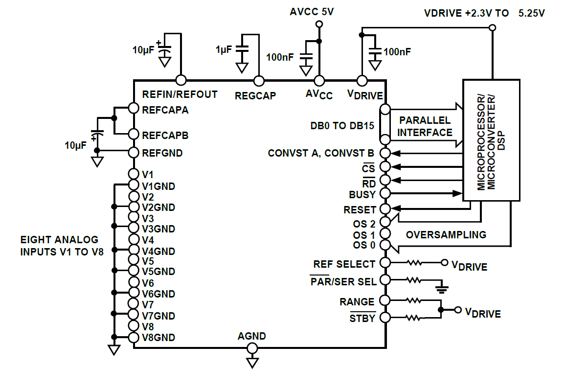
Figure 14. Typical Connection Diagram
Power-Saving Modes
The FT7606BSTZ-xx features two power-down modes: standby mode and shutdown mode. The STBY pin controls whether the FT7606BSTZ-xx operates in normal mode or one of the two power-down modes. When the STBY pin is at a low level, the power-down mode is selected based on the state of the RANGE pin. Table 2 illustrates the configurations required to select the desired power-down mode.When the chip is in standby mode, the maximum current consumption is 7mA, and the power-up time is approximately 100µs due to the need for charging the capacitors on the REFCAPA and REFCAPB pins. In standby mode, the on-chip reference and voltage regulator remain powered, while the amplifiers and ADC core are powered down.
Table 2. Power-Saving Mode Selection
| Power-saving mode | STBY | RANGE |
| Standby | 0 | 1 |
| Shutdown | 0 | 0 |
When the FT7606BSTZ-xx is in shutdown mode, the maximum current consumption is 6mA, and the power-up time is approximately 13ms (in external reference mode). In shutdown mode, all circuits are turned off. When the FT7606BSTZ-xx is powered up from shutdown mode, a RESET signal must be applied to the FT7606BSTZ-xx after the required power-up time has elapsed.
Conversion Control
● Synchronous Sampling of All Analog Input Channels
The FT7606BSTZ-xx allows simultaneous sampling of all analog input channels. When the two CONVST pins (CONVSTA, CONVSTB) are connected together, all channels are sampled simultaneously. A single CONVST signal is used to control both CONVSTx inputs. The rising edge of this common CONVST signal initiates synchronous sampling of all analog input channels (V1 to V8 of the FT7606BSTZ-xx). The FT7606BSTZ-xx incorporates an on-chip oscillator for performing conversions. The conversion time for all ADC channels is tCONV. When a conversion is in progress, the BUSY signal indicates this to the user. Thus, when a CONVST rising edge is applied, the BUSY signal goes high at the start of the conversion process and remains high throughout the conversion; it goes low upon completion of the conversion. The falling edge of BUSY also indicates that new data is now available for reading from the parallel bus (DB[15:0]), the DOUTA and DOUTB serial data lines, or the parallel byte bus DB[7:0].
● Synchronous Sampling of Two Channel Groups
The FT7606BSTZ-xx also allows analog input channels to be sampled simultaneously in two groups. This can be utilized in power line protection and measurement systems to compensate for phase differences introduced by PT and CT transformers. In 50Hz systems, this enables phase compensation up to 9°; in 60Hz systems, it allows phase compensation up to 10°. This is achieved by pulsing the two CONVST pins independently, which is only possible when oversampling is not used. CONVSTA is used to initiate simultaneous sampling of the first group of channels (V1 to V4 of the FT7606BSTZ-xx); CONVSTB is used to initiate synchronous sampling on the second group of analog input channels (V5 to V8 of the FT7606BSTZ-xx), as shown in Figure 15. The conversion process starts when the rising edges of the two CONVSTx occur; thus, BUSY goes high on the rising edge of the later CONVSTx signal. Time t5 represents the maximum allowed time between the CONVSTx sampling points. When using two separate CONVSTx signals, the data reading process remains unchanged. Connect all unused analog input channels to AGND. Results from any unused channels are still included in the data read, as all channels are always converted.
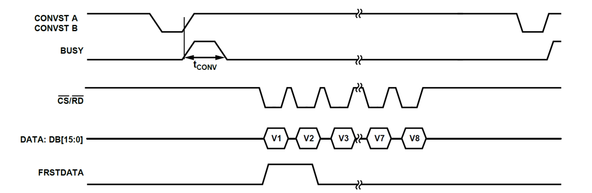
Figure 15. Parallel Mode with Two Channel Groups Synchronously Sampled Using Independent CONVST A and CONVST B Signals
Digital Interface
The FT7606BSTZ-xx provides three interface options: parallel interface, high-speed serial interface, and parallel byte interface. The desired interface mode is selected through the PAR/SER/BYTE SEL and DB15/BYTE SEL pins.
Table 3. Interface Mode Selection
| PAR/SER/BYTE SEL | DB15 | Interface modes |
| 0 | 0 | Parallel interface mode |
| 1 | 0 | Serial interface mode |
| 1 | 1 | Parallel byte interface mode |
● Parallel Interface (PAR/SER/BYTESEL=0)
Data can be read from the FT7606BSTZ-xx via a parallel data bus with standard CS and RD signals. To read data through the parallel bus, the PAR/SER/BYTE SEL pin should be connected to a low level. The CS and RD input signals are internally gated to enable the conversion results onto the data bus. When both CS and RD are at logic low levels, the data lines from DB15 to DB0 are no longer in a high-impedance state.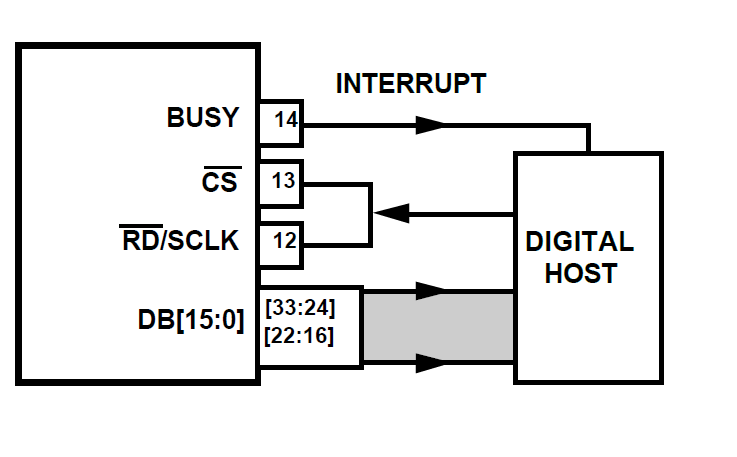
Figure 16. FT7606BSTZ-xx Interface Diagram – Parallel Bus with CS and RD Short-Circuited
The rising edge of the CS input signal places the bus in a tri-state, while the falling edge of the CS input signal takes the bus out of the high-impedance state. CS is the control signal that enables the data lines; it is the feature that allows multiple FT7606BSTZ-xx devices to share the same parallel data bus. The CS signal can be permanently tied to a low level, and the RD signal can be used to access conversion results, as shown in Figure 5. Reading of new data can be performed after the BUSY signal goes low (see Figure 2); alternatively, reading of data from the previous conversion process can be performed while BUSY is high (see Figure 3). The RD pin is used to read data from the output conversion result registers. Applying a sequence of RD pulses to the RD pin of the FT7606BSTZ-xx clocks the conversion results of each channel onto the parallel bus DB[15:0] in ascending order. The first RD falling edge after BUSY goes low clocks out the conversion result of channel V1, the next RD falling edge updates the bus with the V2 conversion result, and so on. On the FT7606BSTZ-xx, the 8th falling edge of RD clocks out the conversion result of channel V8. When the RD signal is at logic low, the data conversion results of each channel can be transmitted to the digital host (DSP, FPGA). When there is only one FT7606BSTZ-xx in a system/board and it does not share the parallel bus, a single control signal from the digital host can be used to read data. The CS and RD signals can be connected together, as shown in Figure 6. In this case, the data bus comes out of tri-state on the CS/RD falling edge. With the CS and RD signals combined, data can be clocked out of the FT7606BSTZ-xx and read by the digital host. In this scenario, CS is used for data frame transmission of each data channel.
● Parallel Byte Mode (PAR/SER/BYTE SEL = 1, DB15 = 1)
The parallel byte interface mode is very similar to the parallel interface mode, except that the conversion result of each channel is read out in two 8-bit transmissions. Therefore, 16 RD pulses are required to read all 8 conversion results from the FT7606BSTZ-xx. To configure the FT7606BSTZ-xx to operate in parallel byte mode, the PAR/SER/BYTE SEL and BYTE SEL/DB15 pins should be connected to a logic high level (see Table 3). In parallel byte mode, DB[7:0] is used to transmit data to the digital host. DB0 is the LSB of the data transmission, and DB7 is the MSB of the data transmission. In parallel byte mode, DB14 functions as an HBEN pin. When DB14/HBEN is connected to a logic high level, the most significant byte (MSB) of the conversion result is output first, followed by the LSB of the conversion result. When DB14 is connected to a logic low level, the LSB of the conversion result is output first, followed by the MSB of the conversion result. The FRSTDATA pin remains high until the full 16-bit conversion result of V1 is read from the FT7606BSTZ-xx.
● Serial Interface (PAR/SER/BYTE SEL = 1)
To read data from the FT7606BSTZ-xx via the serial interface, the PAR/SER/BYTE SEL pin must be connected to a high level. The CS and SCLK signals are used to transmit data from the FT7606BSTZ-xx. The FT7606BSTZ-xx features two serial data output pins, DOUTA and DOUTB. Data can be read from the FT7606BSTZ-xx using either one or both DOUT lines. For the FT7606BSTZ-xx, conversion results from channels V1 to V4 first appear on DOUTA, while conversion results from channels V5 to V8 first appear on DOUTB. The falling edge of CS takes the data output lines DOUTA and DOUTB out of tri-state and latches the MSB of the conversion results. The rising edge of SCLK clocks all subsequent data bits to the serial data outputs, DOUTA and DOUTB. The CS input can remain low throughout the entire serial read operation, or it can be pulsed to frame each channel read for 16 SCLK cycles. Figure 17 shows the reading of 8 synchronous conversion results using the two DOUT lines on the FT7606BSTZ-xx.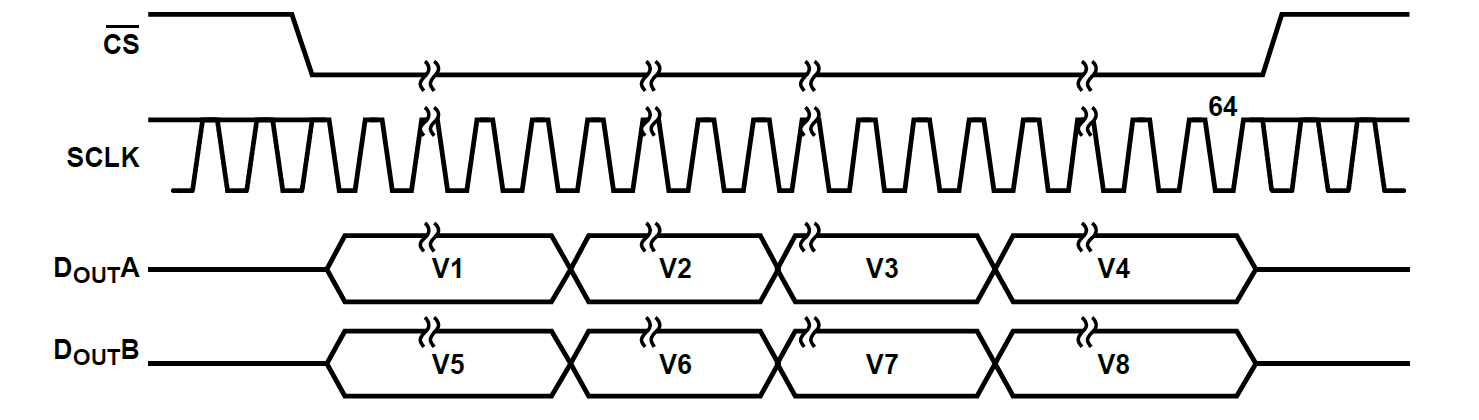 Figure 17. FT7606BSTZ-xx Serial Interface with Dual DOUT Lines
In this scenario, a 64-SCLK transmission is used to access data from the FT7606BSTZ-xx, with CS remaining low to enable the entire 64-SCLK cycle frame. It is also possible to use only one DOUT line for data retrieval; in this case, it is recommended to use DOUTA to access all conversion data, as channel data is output in ascending order. To access all 8 conversion results on a single DOUT line of the FT7606BSTZ-xx, a total of 128 SCLK cycles are required. These 128 SCLK cycles can be framed by a single CS signal, or each group of 16 SCLK cycles can be individually framed by CS signals. The disadvantage of using only one DOUT line is reduced throughput when reading data after conversion. Unused DOUT lines should not be connected in serial mode. For the FT7606BSTZ-xx, if DOUTB is used as the single DOUT line, the channel results are output in the following order: V5, V6, V7, V8, V1, V2, V3, V4. However, after reading V5 on DOUTB, the FRSTDATA indicator returns to a low level. Figure 7 shows the timing diagram for reading data from one channel of the FT7606BSTZ-xx in serial mode (framed by the CS signal). The SCLK input signal provides the clock source for serial read operations. A low CS level enables access to the FT7606BSTZ-xx data. The falling edge of CS takes the bus out of tri-state and clocks out the MSB of the 16-bit conversion result. This MSB is valid on the first falling edge after the CS falling edge. The subsequent 15 data bits are clocked out of the FT7606BSTZ-xx on the rising edges of SCLK. Data is valid on the falling edges of SCLK. Sixteen clock cycles must be provided to the FT7606BSTZ-xx to access each conversion result. The FRSTDATA output signal indicates when the first channel (V1) is being read back. When the CS input is high, the FRSTDATA output pin is in tri-state. In serial mode, the falling edge of CS takes FRSTDATA out of tri-state and sets the FRSTDATA pin high, indicating that the result from V1 is available on the DOUTA output data line. The FRSTDATA output returns to a logic low after the 16th SCLK falling edge. If all channels are read on DOUTB, the FRSTDATA output does not go high when V1 is output on this serial data output pin. It only goes high when V1 is available on DOUTA (which corresponds to when V5 is available on DOUTB of the FT7606BSTZ-xx).
Read During Conversion
Data can be read from the FT7606BSTZ-xx while BUSY is high and a conversion is in progress. This has minimal impact on the converter’s performance and enables faster throughput rates. Parallel, parallel byte, or serial reads can be performed during conversion, with or without oversampling. Figure 3 shows the timing diagram for reads while BUSY is high in parallel or serial mode. When using a serial interface with VDRIVE above 4.75V, reading during conversion allows full throughput rate to be achieved. Data can be read from the FT7606BSTZ-xx at any time except on the falling edge of BUSY, as this is when the output data registers are updated with new conversion data. In such cases, the time requirement t6 shown in Table 3 must be met.
Digital Filter
The FT7606BSTZ-xx incorporates an optional digital first-order sinc filter, suitable for applications requiring slower throughput rates, higher signal-to-noise ratio (SNR), or extended dynamic range. The oversampling ratio of the digital filter is controlled by the oversampling pins, OS[2:0], where OS2 serves as the MSB control bit and OS0 as the LSB control bit. Table 4 provides the oversampling bit decoding for selecting different oversampling rates. The OS pins are latched on the falling edge of BUSY, which sets the oversampling rate for the next conversion. In addition to the oversampling functionality, the output results are decimated to 16-bit resolution.
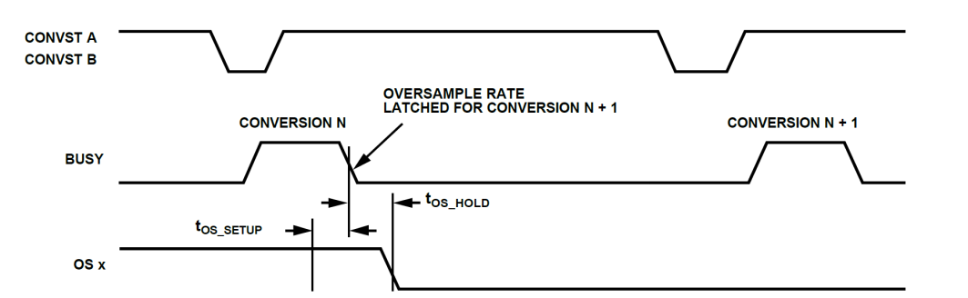
Figure 18. OS x Pin Timing
Table 4. Oversampling Bit Decoding
| OS[2:0] | Oversampling ratio | SNR @ 5V range (dB) | SNR @ 10V range (dB) | 3 dB bandwidth @ 5V range (kHz) | 3 dB bandwidth @ 10V range (kHz) | Maximum throughput CONVST frequency (kHz) |
| 000 | No OS | 88.5 | 89 | 15 | 22 | 200 |
| 001 | 2 | 90.3 | 91 | 15 | 22 | 100 |
| 010 | 4 | 91.7 | 92.5 | 13.7 | 18.5 | 50 |
| 011 | 8 | 93.2 | 93.4 | 10.3 | 11.9 | 25 |
| 100 | 16 | 94.8 | 95 | 6 | 6 | 12.5 |
| 101 | 32 | 95.1 | 95.6 | 3 | 3 | 6.25 |
| 110 | 64 | 95.8 | 96.1 | 1.5 | 1.5 | 3.125 |
| 111 | Invalid |
If the OS pins are set to select an oversampling (OS) ratio of 8, the next rising edge of CONVSTx will acquire the first sample for each channel, with the remaining 7 samples for all channels acquired using internally generated sampling signals. These samples are then averaged to enhance signal-to-noise ratio (SNR) performance. Typical SNR performances for ±10V and ±5V ranges are shown. As indicated in Table 4, SNR improves with increasing OS ratio. However, higher OS ratios result in lower 3dB frequencies and reduced allowable sampling frequencies. In applications requiring a sampling frequency of 10kSPS, an OS ratio of up to 16 can be used. In this scenario, the application benefits from improved SNR, but the input 3dB bandwidth is limited to approximately 6kHz. When oversampling is enabled, the CONVSTA and CONVSTB pins must be connected together/driven synchronously. Activating the oversampling function extends the duration of the BUSY high period during conversion. The actual BUSY high duration depends on the selected oversampling ratio: higher ratios result in longer BUSY high periods or total conversion times. As illustrated in Figure 19, conversion time increases with the oversampling ratio, and the BUSY signal duration extends accordingly for different ratios. For example, a sampling frequency of 10kSPS yields a 100µs period. Figures 21 and 22 demonstrate OS×2 and OS×4 configurations; in the 10kSPS example, sufficient cycle time exists to further increase the oversampling ratio for greater SNR improvements. For applications with an initial sampling or throughput rate of 200kSPS, enabling oversampling requires reducing the throughput rate to accommodate longer conversion times and allow for data reading. To achieve the fastest possible throughput with oversampling enabled, read operations can be performed during the BUSY high period. The falling edge of BUSY is used to update the output data registers with new conversion results; therefore, reading conversion data should be avoided during this edge.
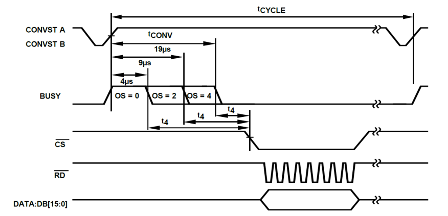
Figure 19. No Oversampling, 2x Oversampling, and 4x Oversampling – Read After Conversion
Figures 20 to 26 illustrate the impact of oversampling on code distribution in DC histograms. As the oversampling ratio increases, code spread decreases. When the FT7606BSTZ-xx is set to oversampling mode, it functions equivalently to adding a digital filter after the ADC. Different oversampling ratios and CONVST sampling frequencies result in distinct digital filter frequency distributions.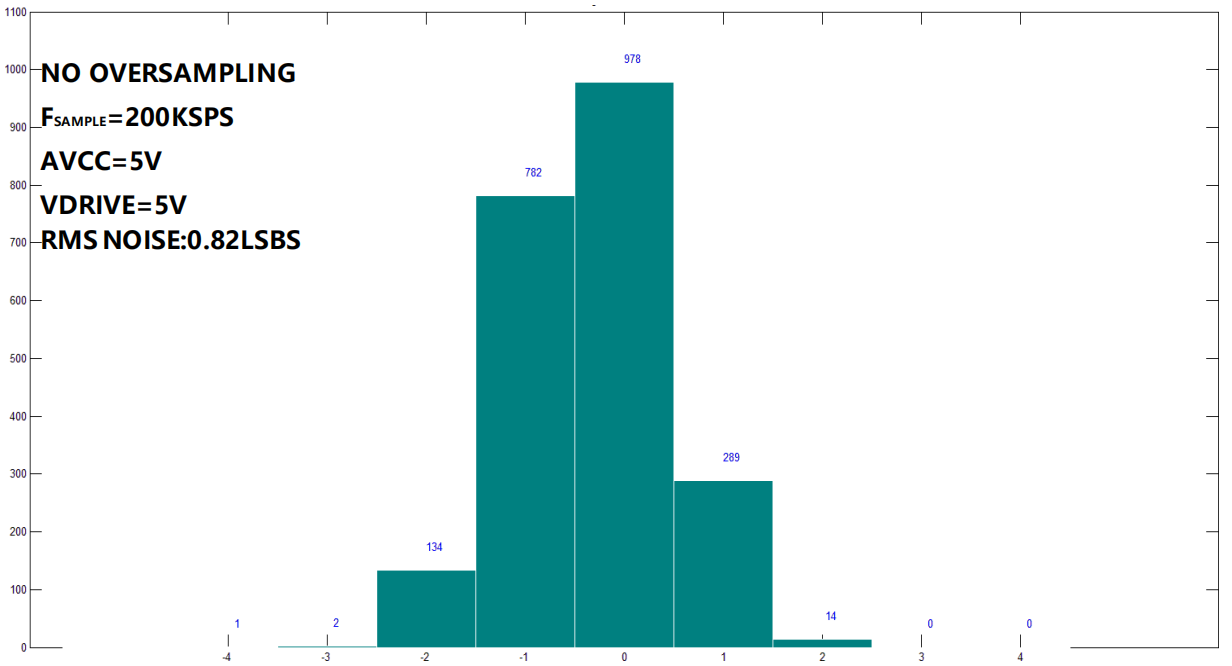
Figure 20. Histogram Data – No OS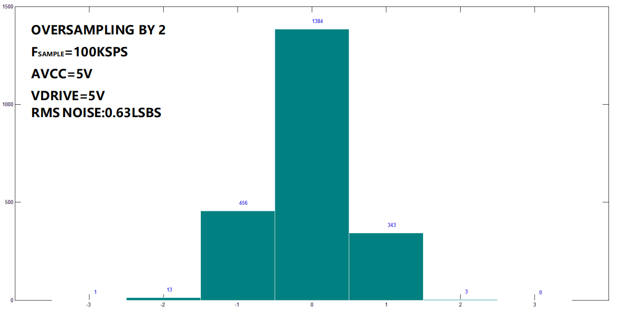
Figure 21. Histogram Data – OS × 2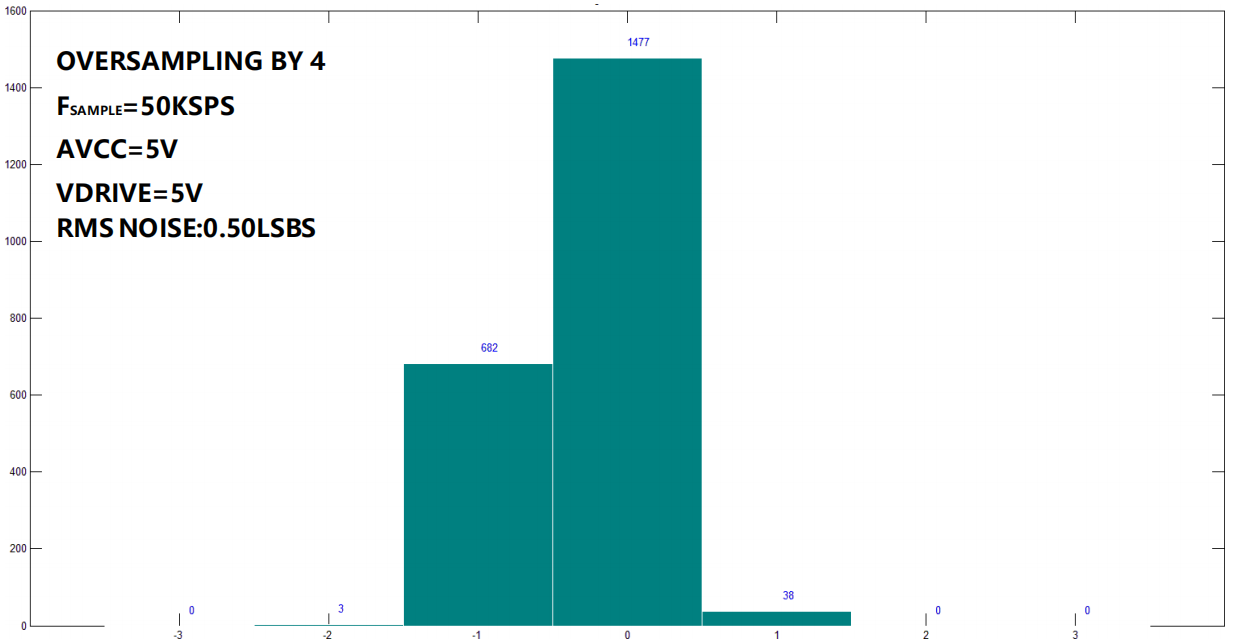
Figure 22. Histogram Data – OS × 4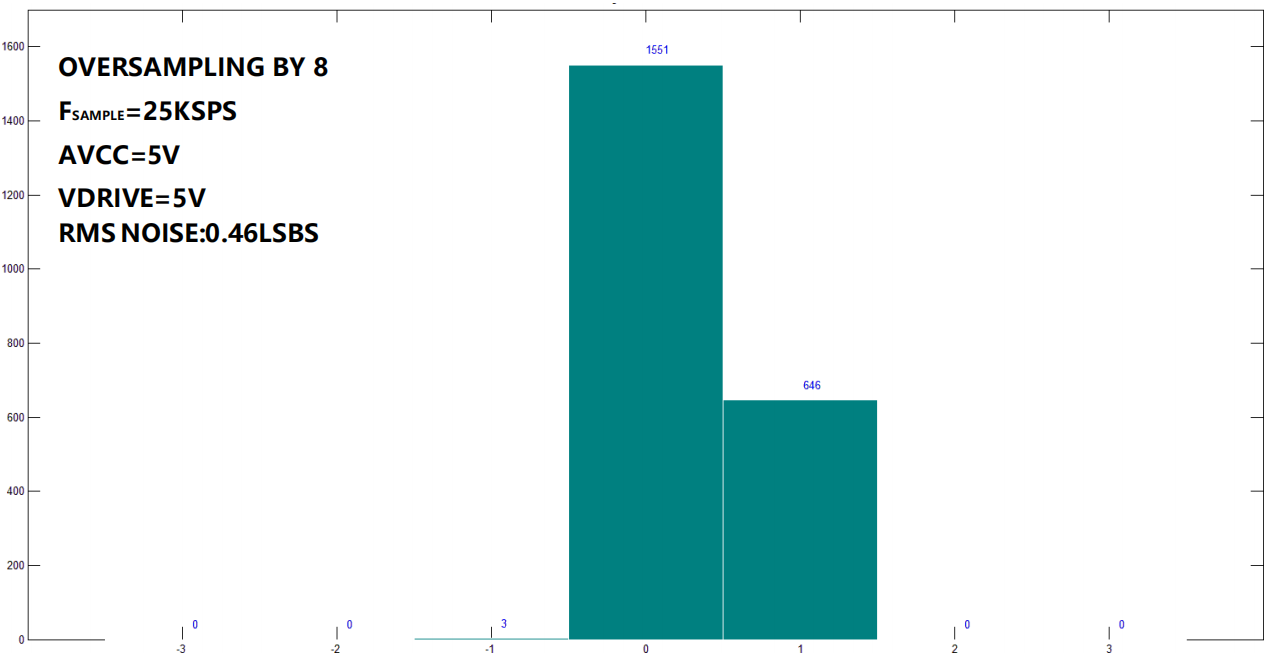
Figure 23. Data – OS × 8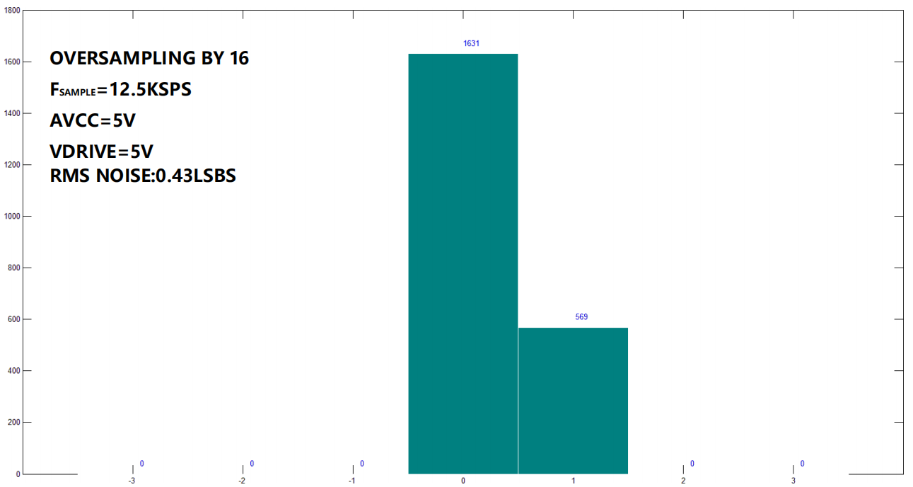
Figure 24. Histogram Data – OS × 16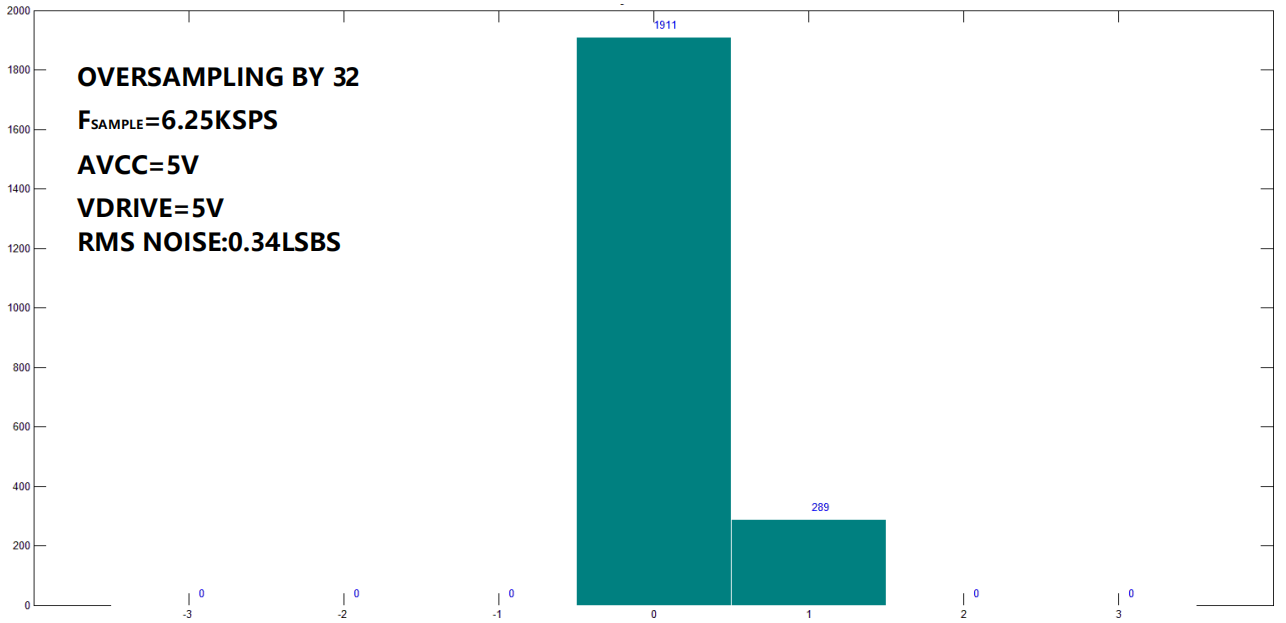
Figure 25. Histogram Data – OS × 32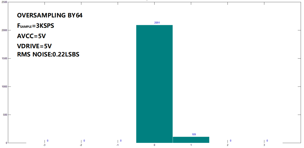
Figure 26. Histogram Data – OS × 64
Layout Guidelines
When designing a printed circuit board (PCB) for applications using the FT7606BSTZ-xx, the analog and digital sections should be separated and confined to different areas of the board. At least one ground plane should be used; it can be a solid plane or split between the digital and analog sections. In the case of split planes, the digital and analog ground planes should be connected at only one point, preferably as close as possible to the FT7606BSTZ-xx. If the FT7606BSTZ-xx is part of a system where multiple devices require analog-to-digital grounding, the connection should still be made at a single point: a star grounding point should be established as close as possible to the FT7606BSTZ-xx. A good connection to the ground plane is essential. Avoid sharing a single connection among multiple ground pins. For each ground pin, use separate or multiple vias to the ground plane. Do not route digital traces under the device, as this can couple noise into the die. The analog ground plane should be allowed to run under the FT7606BSTZ-xx to prevent noise coupling. Fast-switching signals such as CONVSTA, CONVSTB, or clocks should be shielded with digital ground to avoid radiating noise to other parts of the board, and they should not be routed near analog signal paths. Avoid crossing digital and analog signals. Traces on adjacent layers of the board should run at right angles to each other to reduce feedthrough effects through the board. The power supply traces for the AVCC and VDRIVE pins on the FT7606BSTZ-xx should use the largest possible trace size to provide a low-impedance path and minimize the impact of voltage spikes on the power lines. When possible, use power planes and ensure a good connection between the FT7606BSTZ-xx power pins and the power planes on the board. Use one or more vias for each power pin. Proper decoupling is also critical for reducing the power supply impedance of the FT7606BSTZ-xx and minimizing the amplitude of power supply spikes. Decoupling capacitors should be placed as close as possible (ideally, directly opposite) to these pins and their corresponding ground pins. Locate the decoupling capacitors for the REFIN/REFOUT pin, as well as the REFCAPA and REFCAPB pins, as close as possible to their respective FT7606BSTZ-xx pins; furthermore, they should be placed on the same board layer as the FT7606BSTZ-xx device when possible. Figure 27 shows the recommended decoupling on the top layer of the FT7606BSTZ-xx board. Figure 28 shows the bottom-layer decoupling for the four AVCC pins and the VDRIVE pin. The 100nF ceramic capacitors for the AVCC pins are placed near their respective device pins, and a single 100nF capacitor can be shared between pin 37 and pin 38.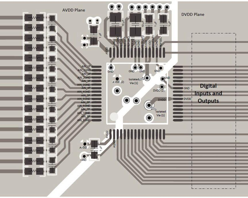 Figure 27. Top-Layer Layout for All Pins
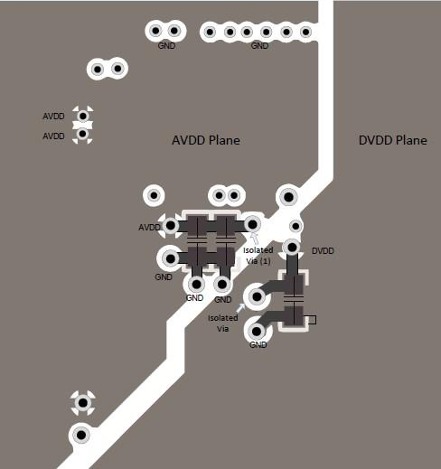
Figure 28. Bottom-Layer Layout
In a system containing multiple FT7606BSTZ-xx devices, a symmetrical layout between the FT7606BSTZ-xx devices is crucial to ensure performance matching among them. Figure 29 shows a layout with two FT7606BSTZ-xx devices. The AVCC power plane is on the right side of both devices, and the VDRIVE power trace is on the left side of both devices. The reference chip is located between the two devices, with the reference voltage trace running north to pin 42 of U1 and south to pin 42 of U2. A solid ground plane is adopted. These symmetrical layout principles also apply to systems containing more than two FT7606BSTZ-xx devices. The FT7606BSTZ-xx devices can be placed in the north-south direction, with the reference voltage located between the devices and the reference traces running in the north-south direction, as shown in Figure 29.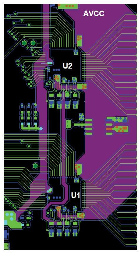
Figure 29. FT7606BSTZ-xx Multi-Device Layout – Top Layer and Power Layer
Package Dimensions and Structure
Device Ordering Information
| Model number | Temperature range | Package | Packaging |
| FT7606BSTZ | -40℃~85℃ | LQFP64 | Tray of 1280 |
| FT7606BSTZ-M | -40℃~125℃ | LQFP64 | Tray of 1280 |
Важное уведомление
Performance figures, data and any illustrative material provided in this data sheet are typical and must be specifically confirmed in writing by F-tone Networks before they are applicable to any particular order or contract. In accordance with the F-tone Networks policy of continuous improvement specifications may change without notice.
The publication of information in this data sheet does not imply freedom from patent or other protective rights of F-tone Networks or other. Further details are available from any F-tone Networks sales representative.
Power and Wavelength Testing
Test the signal delivering strength and wavelength, to ensure the signal decoding capacity of the receiver, and the wavelength remains consistent from the transmitter to the receiver.
Traffic Testing
Test the bit error rate and packet loss rate, to make them meet the corresponding standards and ensure the performance of transceivers.
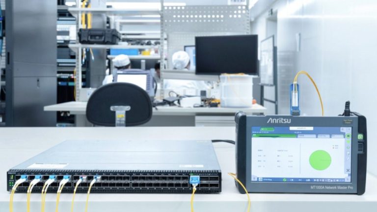
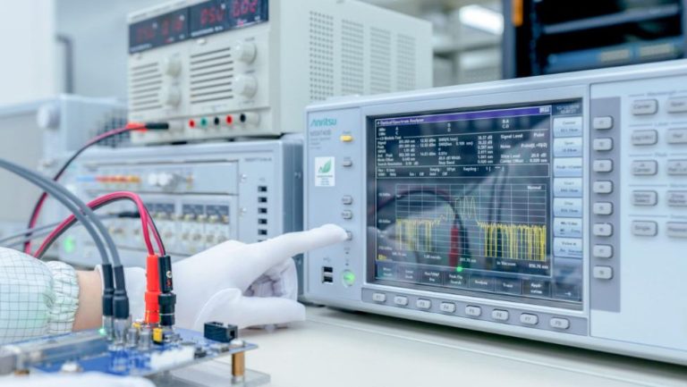
Optical Performance Testing
Test the transceivers’ eye diagram situation, receiving sensitivity, extinction ratio, wavelength, light-emitting, light-receiving, current and voltage, to ensure the signal quality, stability and reliability of the transmission.
End Face Testing
Check the end face of the transceivers and keep them clean for more stable data transmission, better performance, and durability.

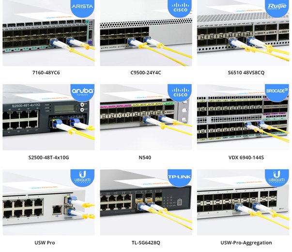
Compatible Brands:
Cisco | Juniper | Arista | Brocade |HPE ProCurve | HPE Aruba | HPE BladeSystem | HPE H3C | H3C | Dell | Extreme | HW | Generic | F-tone | Intel
Netgear | IBM | NVIDIA/Mellanox (Ethernet) | Ciena | Fortinet | Avago | Avaya | Alcatel-Lucent | D-Link | F5 | Ubiquiti | Mikrotik |Broadcom…..